- 您现在的位置:买卖IC网 > Sheet目录489 > NTJS4151PT1 (ON Semiconductor)MOSFET P-CH 20V 3.3A SOT-363
�� �
�
�NTJS4151P�
�Trench� Power� MOSFET�
�?� 20� V,� ?� 4.2� A,� Single� P� ?� Channel,� SC� ?� 88�
�Features�
�?� Leading� Trench� Technology� for� Low� R� DS(ON)� Extending� Battery� Life�
�?� SC� ?� 88� Small� Outline� (2x2� mm)� for� Maximum� Circuit� Board�
�Utilization,� Same� as� SC� ?� 70� ?� 6�
�?� Gate� Diodes� for� ESD� Protection�
�?� Pb� ?� Free� Package� is� Available�
�Applications�
�?� High� Side� Load� Switch�
�?� Cell� Phones,� Computing,� Digital� Cameras,� MP3s� and� PDAs�
�V� (BR)DSS�
�?� 20� V�
�http://onsemi.com�
�R� DS(on)� Typ�
�47� m� W� @� ?� 4.5� V�
�70� m� W� @� ?� 2.5� V�
�180� m� W� @� ?� 1.8� V�
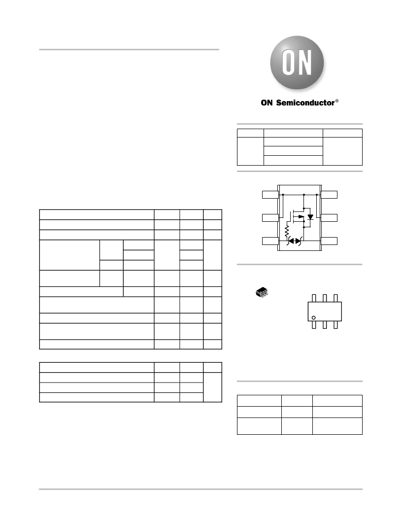
�SC� ?� 88� (SOT� ?� 363)�
�I� D� Max�
�?� 4.2� A�
�D�
�1�
�6�
�D�
�MAXIMUM� RATINGS� (T� J� =� 25� °� C� unless� otherwise� stated)�
�Parameter�
�Drain� ?� to� ?� Source� Voltage�
�Symbol�
�V� DSS�
�Value�
�?� 20�
�Unit�
�V�
�D�
�2�
�5�
�D�
�Gate� ?� to� ?� Source� Voltage�
�Continuous� Drain�
�Current� (Note� 1)�
�Steady�
�State�
�T� A� =� 25� °� C�
�T� A� =� 85� °� C�
�V� GS�
�I� D�
�±� 12�
�?� 3.3�
�?� 2.4�
�V�
�A�
�G�
�3�
�Top� View�
�4�
�S�
�t� ≤� 5s�
�T� A� =� 25� °� C�
�?� 4.2�
�Power� Dissipation�
�(Note� 1)�
�Steady�
�State�
�T� A� =� 25� °� C�
�P� D�
�1.0�
�W�
�MARKING� DIAGRAM� &�
�PIN� ASSIGNMENT�
�Pulsed� Drain� Current� t� p� =� 10� m� s�
�Operating� Junction� and� Storage� Temperature�
�Source� Current� (Body� Diode)�
�Lead� Temperature� for� Soldering� Purposes�
�(1/8”� from� case� for� 10� s)�
�I� DM�
�T� J� ,�
�T� STG�
�I� S�
�T� L�
�?� 10�
�?� 55� to�
�150�
�?� 1.3�
�260�
�A�
�°� C�
�A�
�°� C�
�1�
�SC� ?� 88/SOT� ?� 363�
�CASE� 419B�
�6�
�1�
�D�
�D�
�D�
�TY� M� G�
�G�
�D�
�S�
�G�
�ESD�
�Human� Body� Model� (HBM)�
�ESD�
�4000�
�V�
�TY�
�=� Device� Code�
�THERMAL� RESISTANCE� RATINGS� (Note� 1)�
�M�
�G�
�=� Date� Code�
�=� Pb� ?� Free� Package�
�Parameter�
�Junction� ?� to� ?� Ambient� –� Steady� State�
�Junction� ?� to� ?� Ambient� ?� t� ≤� 5� s�
�Symbol�
�R� q� JA�
�R� q� JA�
�Max�
�125�
�75�
�Unit�
�°� C/W�
�(Note:� Microdot� may� be� in� either� location)�
�ORDERING� INFORMATION�
�3000� /� Tape� &� Reel�
�NTJS4151PT1G�
�Junction� ?� to� ?� Lead� –� Steady� State� R� q� JL� 45�
�Maximum� ratings� are� those� values� beyond� which� device� damage� can� occur.�
�Maximum� ratings� applied� to� the� device� are� individual� stress� limit� values� (not�
�normal� operating� conditions)� and� are� not� valid� simultaneously.� If� these� limits� are�
�exceeded,� device� functional� operation� is� not� implied,� damage� may� occur� and�
�reliability� may� be� affected.�
�1.� Surface� mounted� on� FR4� board� using� 1� in� sq� pad� size�
�(Cu� area� =� 1.127� in� sq� [1� oz]� including� traces).�
�Device� Package� Shipping� ?�
�NTJS4151PT1� SC� ?� 88� 3000� /� Tape� &� Reel�
�SC� ?� 88�
�(Pb� ?� Free)�
�?For� information� on� tape� and� reel� specifications,�
�including� part� orientation� and� tape� sizes,� please�
�refer� to� our� Tape� and� Reel� Packaging� Specifications�
�Brochure,� BRD8011/D.�
�?� Semiconductor� Components� Industries,� LLC,� 2006�
�February,� 2006� ?� Rev.� 1�
�1�
�Publication� Order� Number:�
�NTJS4151P/D�
�发布紧急采购,3分钟左右您将得到回复。
相关PDF资料
NTJS4160NT1G
MOSFET N-CH 30V 1.8A SC88-6
NTJS4405NT4G
MOSFET N-CH 25V 1A SOT-363
NTK3043NT5G
MOSFET N-CH 20V 210MA SOT-723
NTK3134NT5G
MOSFET N-CH 20V 750MA SOT-723
NTK3139PT5G
MOSFET P-CH 20V 660MA SOT-723
NTK3142PT1G
MOSFET P-CHAN 260MA 20V SOT-723
NTLGD3502NT2G
MOSFET N-CH DUAL 20V 6-DFN
NTLGF3402PT2G
MOSFET P-CH 20V 2.3A 6-DFN
相关代理商/技术参数
NTJS4151PT1G
功能描述:MOSFET -20V -4.2A P-Channel RoHS:否 制造商:STMicroelectronics 晶体管极性:N-Channel 汲极/源极击穿电压:650 V 闸/源击穿电压:25 V 漏极连续电流:130 A 电阻汲极/源极 RDS(导通):0.014 Ohms 配置:Single 最大工作温度: 安装风格:Through Hole 封装 / 箱体:Max247 封装:Tube
NTJS4160N
制造商:ONSEMI 制造商全称:ON Semiconductor 功能描述:High Efficiency DC-DC Converters
NTJS4160NT1G
功能描述:MOSFET NFET 30V 3.2A 60MOHM RoHS:否 制造商:STMicroelectronics 晶体管极性:N-Channel 汲极/源极击穿电压:650 V 闸/源击穿电压:25 V 漏极连续电流:130 A 电阻汲极/源极 RDS(导通):0.014 Ohms 配置:Single 最大工作温度: 安装风格:Through Hole 封装 / 箱体:Max247 封装:Tube
NTJS4405N
制造商:ONSEMI 制造商全称:ON Semiconductor 功能描述:Small Signal MOSFET 25 V, 1.2 A, Single, N−Channel, SC−88
NTJS4405NT1
功能描述:MOSFET 25V 1.2A N-Channel RoHS:否 制造商:STMicroelectronics 晶体管极性:N-Channel 汲极/源极击穿电压:650 V 闸/源击穿电压:25 V 漏极连续电流:130 A 电阻汲极/源极 RDS(导通):0.014 Ohms 配置:Single 最大工作温度: 安装风格:Through Hole 封装 / 箱体:Max247 封装:Tube
NTJS4405NT1G
功能描述:MOSFET 25V 1.2A N-Channel RoHS:否 制造商:STMicroelectronics 晶体管极性:N-Channel 汲极/源极击穿电压:650 V 闸/源击穿电压:25 V 漏极连续电流:130 A 电阻汲极/源极 RDS(导通):0.014 Ohms 配置:Single 最大工作温度: 安装风格:Through Hole 封装 / 箱体:Max247 封装:Tube
NTJS4405NT4
功能描述:MOSFET 25V 1.2A N-Channel RoHS:否 制造商:STMicroelectronics 晶体管极性:N-Channel 汲极/源极击穿电压:650 V 闸/源击穿电压:25 V 漏极连续电流:130 A 电阻汲极/源极 RDS(导通):0.014 Ohms 配置:Single 最大工作温度: 安装风格:Through Hole 封装 / 箱体:Max247 封装:Tube
NTJS4405NT4G
功能描述:MOSFET 25V 1.2A N-Channel RoHS:否 制造商:STMicroelectronics 晶体管极性:N-Channel 汲极/源极击穿电压:650 V 闸/源击穿电压:25 V 漏极连续电流:130 A 电阻汲极/源极 RDS(导通):0.014 Ohms 配置:Single 最大工作温度: 安装风格:Through Hole 封装 / 箱体:Max247 封装:Tube